Chapter 26: GPU Systems Programming & Memory-Mapped I/O
So far, we have used the GPU only through the CUDA API. cudaMalloc returns a pointer,
cudaMemcpy moves data, and a kernel launch with <<<grid, block>>> returns to the host after
a few microseconds while the kernel continues to run on the device. In Chapter 6, we measured a
launch at 3.77 µs. Because the CPU and the GPU are separate devices, a launch cannot be an
ordinary function call: the CPU must deliver the work to the GPU through the hardware that
connects them. The driver is the software that operates the GPU on behalf of programs; in section
26.7 we show that it consists of 2 parts. In this chapter, we study the hardware that connects the
CPU and the GPU and the way the driver uses it.
We start with the physical addresses through which a CPU reaches any device, and with the way the operating system finds a GPU and the address ranges that the GPU occupies. We then look at the two ways in which the CPU and the GPU exchange information: small stores into the GPU’s registers, called memory-mapped I/O, and bulk transfers that the GPU performs by itself, called direct memory access. With these mechanisms in place, we follow a kernel launch from the CPU to the GPU’s streaming multiprocessors (SMs), the processors that run the threads of a kernel, and we build a working model of the mechanism with 2 CPU threads, in C++ and in Rust.
This chapter covers
- physical addresses, and memory-mapped I/O: devices that answer to addresses
- PCIe devices, their configuration space and their base address registers (BARs)
- Three ways to attach a GPU: a discrete card on PCIe, an integrated GPU presented as a PCIe function, and an integrated GPU described by the device tree
- the control path (MMIO) and the data path (DMA), and why they differ
- cached, write-combined and device memory, measured from the CPU
- work rings and doorbells: how a kernel launch reaches the GPU without a system call
- the order of writes before a doorbell, and the errors that a wrong order causes
- the IOMMU, which checks every address a device uses
- the kernel-mode and user-mode drivers, and how to observe all of it on Linux
The code of the chapter is in
code/ch17_systems/
for C++ and in
code/oxide/ch17_systems/
for Rust. Neither needs root, the administrator account of Linux: everything we show in the
chapter can be read by an ordinary user.
26.1 The GPU is a device on a bus
26.1.1 Physical addresses and memory-mapped I/O
A processor names every byte it reads or writes by a number, its address. The addresses that a program uses are virtual: each process has its own, and the same virtual address in 2 processes may name 2 different bytes. The processor’s memory management unit (MMU) translates each virtual address into a physical address: the number that leaves the core and travels on the chip’s internal buses. The MMU translates in units of pages, blocks of usually 4 KiB, and it reads the translation of each page from the page tables that the operating system keeps. For example, with pages of 4 KiB = 0x1000 bytes, the virtual address 0x7F12_3456 lies in virtual page 0x7F123 at offset 0x456. If the page table maps that page to physical page 0x80042, the physical address is 0x8004_2456: the page number changes, and the offset within the page stays. The set of all physical addresses is the physical address space. On a 64-bit Arm or x86 machine it spans far more numbers than the machine has bytes of memory, and most physical addresses lead nowhere.
The chip’s interconnect, the network of internal buses that joins the cores to everything else, decides where each physical address goes. Some ranges lead to the memory controllers and so to DRAM, the main memory. Other ranges lead to devices: a disk controller, a network card, the GPU. A register of a device is a small storage location inside the device, often 4 bytes, whose contents control the device or report its state.
To see how a device can be reached by address, consider a small machine that we invent for the purpose, whose physical addresses run from 0x0000 to 0xFFFF. Its interconnect sends the addresses 0x0000 to 0x7FFF to DRAM, and the addresses 0x8000 to 0x80FF to a device with 64 registers of 4 bytes each. A store of the value 1 to address 0x0010 writes 1 into DRAM, and a later load from 0x0010 returns the 1. A store of the value 1 to address 0x8004 instead reaches the device: 0x8004 − 0x8000 = 4 bytes past the start of its range, which is register 1. If register 1 is the device’s “start” register, the store starts the device. Both stores are the same instruction; only the address differs.
Definition 26.1 Memory-mapped I/O. Memory-mapped I/O, or MMIO, is the arrangement in which a range of physical addresses leads to the registers of a device, so that a load from one of those addresses reads a register and a store writes one. The device is operated with the same load and store instructions that work on memory, and the address alone decides whether an instruction reaches DRAM or a device.
Example. In the small machine above, a store to 0x8004 writes register 1 of the device, while a store to 0x0010 writes DRAM.
Figure 26.1 shows the ranges that matter to this chapter on a Jetson Orin NX, a machine whose
GPU is built into the processor chip. They come from the machine’s device tree, a
description of the hardware that the firmware, the program stored on the board that starts
the machine, hands to Linux at boot. The device tree holds 1 node for each built-in device,
and each node holds named properties. The property reg lists the physical addresses of the
device’s registers.
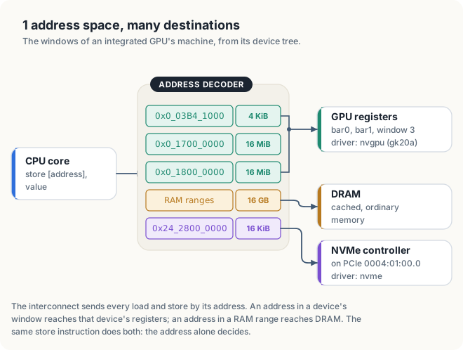
The GPU’s node in that device tree holds 3 pairs of (address, size). Read as raw
bytes, its reg property is:
$ xxd -g4 /sys/firmware/devicetree/base/bus@0/gpu@17000000/reg
00000000: 00000000 17000000 00000000 01000000  ................
00000010: 00000000 18000000 00000000 01000000  ................
00000020: 00000000 03b41000 00000000 00001000  ................
Each number in the property is written as 2 words of 32 bits, high word first, and each row holds an address followed by a size. A window is a range of physical addresses that leads to 1 device. The first row therefore describes a window at 0x1700_0000 of 0x0100_0000 = 16,777,216 bytes, or 16 MiB. The second row describes another 16 MiB window at 0x1800_0000, and the third a window of 0x1000 = 4,096 bytes at 0x03B4_1000.
The word kernel has 2 meanings in this chapter. The operating-system kernel is the part of the
operating system that runs with full privileges and controls the hardware; we call it “the
kernel”. A GPU kernel, the function that runs on the GPU, appears mostly in the phrase “kernel
launch”. The Linux kernel’s binding for this family of GPUs, the document that states what
the device tree must say about such a device, names the first 2 windows bar0 and bar1, after
the BARs of a PCIe GPU that we introduce in section 26.2.
A store by the CPU to 0x1700_0000 + \(r\) writes the GPU’s register at offset \(r\) of
bar0. The driver, not a program, decides which offsets to touch; in section 26.7 we show how the
operating system keeps ordinary programs away from these addresses.
26.1.2 PCIe: links, functions and addresses
Most devices in a computer are attached to the processor chip through PCIe (PCI Express), the standard connection for expansion devices. In Section 4.1.2, we described its physical side: a link of 1 to 16 lanes, each lane a pair of wires in each direction, carrying about 2 GB/s each way per lane in generation 4.0 and 4 GB/s in 5.0.
In this chapter, we need its logical side. PCIe carries transactions, packets with a type, an address and data. A CPU store to an address inside a device’s window becomes a memory write transaction that travels down the link. A CPU load becomes a memory read transaction, and the device answers with a completion packet that carries the data back. For example, a CPU store of the 4-byte value 1 to offset 0x10 of a device’s window becomes 1 packet that says “memory write, address = window start + 0x10, data = 1”. A CPU load from the same address becomes 2 packets: a “memory read, address = window start + 0x10, length 4” that travels to the device, and a completion with the 4 bytes that travels back. The root complex is the part of the processor chip that turns the CPU’s loads and stores into transactions and back; each of its connectors is a root port. A device at the end of a link is an endpoint.
Each endpoint holds one or more functions, logical devices with their own registers. A
function is named by 4 numbers, written domain:bus:device.function. A domain is 1 separate
tree of PCIe buses, here 1 per root port, and a bus is 1 level of links within that tree. An
NVMe drive is a solid-state disk that is attached by PCIe and follows the NVM Express
standard. The NVMe drive of the same machine is 0004:01:00.0, domain 4, bus 1, device 0,
function 0. lspci lists every function the kernel found:
$ lspci                                               # Orin NX
0001:00:00.0 PCI bridge: NVIDIA Corporation Device 229e (rev a1)
0001:01:00.0 Network controller: Realtek ... RTL8822CE 802.11ac PCIe Wireless Network Adapter
0004:00:00.0 PCI bridge: NVIDIA Corporation Device 229c (rev a1)
0004:01:00.0 Non-Volatile memory controller: Samsung Electronics Co Ltd Device a80c
0008:00:00.0 PCI bridge: NVIDIA Corporation Device 229c (rev a1)
0008:01:00.0 Ethernet controller: Realtek ... RTL8111/8168/8411 PCI Express Gigabit Ethernet
The machine has 3 root ports in use, each shown as a PCI bridge, a function that connects 1 bus to the next, on bus 0 of its own domain, with 1 device behind each: a Wi-Fi card, an NVMe drive and an Ethernet controller. The GPU is not in the list: on this machine it is not a PCIe device at all.
26.1.3 Discrete and integrated GPUs
A discrete GPU is a separate card with its own memory, joined to the CPU by a PCIe link (or, on Grace Hopper, by NVLink-C2C, NVIDIA’s link between a CPU chip and a GPU chip). An integrated GPU is built on the same chip as the CPU and uses the same memory. An integrated GPU can be attached in 2 different ways (figure 26.2).
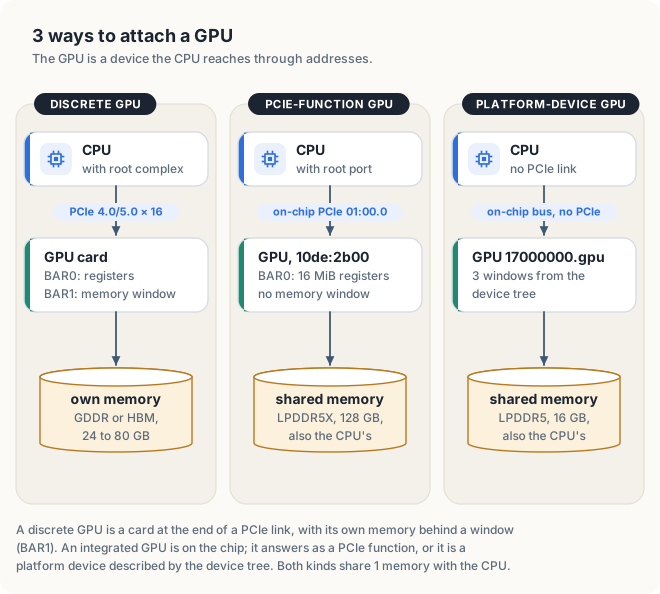
The GPU of figure 26.1 is a platform device: a device that Linux does not discover on a bus but learns about from the device tree, by its fixed register addresses. We call it the platform-device GPU below. An integrated GPU can instead be presented to software as a PCIe function behind an internal root port. The same PCIe machinery that finds a discrete card then finds it. A Jetson AGX Thor attaches its GPU this way, and we call it the PCIe-function GPU:
$ lspci -nn                                           # Jetson AGX Thor
0000:01:00.0 3D controller [0302]: NVIDIA Corporation Device [10de:2b00] (rev a1)
0001:01:00.0 Network controller [0280]: Realtek ... RTL8852CE PCIe 802.11ax Wireless ...
0002:01:00.0 Ethernet controller [0200]: Realtek Semiconductor Co., Ltd. Device [10ec:8126]
0005:01:00.0 Non-Volatile memory controller [0108]: Sandisk Corp WD PC SN5000S M.2 2280 ...
The table puts the 7 GPUs of the earlier chapters side by side. The link column is the path between the CPU and the GPU, with the bandwidth of section 4.1.3. The last column names kinds of DRAM: LPDDR is built for low power and is used in mobile and embedded chips, while GDDR and HBM are built for high bandwidth and are used on graphics cards and data-center GPUs.
| GPU | Attached by | Bandwidth each way | GPU memory |
|---|---|---|---|
| Jetson Orin NX 16 GB | on-chip bus, platform device | none needed: 1 memory | 16 GB LPDDR5, shared |
| Jetson AGX Thor | on-chip, presented as PCIe 01:00.0 | none needed: 1 memory | 128 GB LPDDR5X, shared |
| DGX Spark (GB10) | NVLink-C2C inside 1 package | none needed: 1 memory | 128 GB LPDDR5X, shared |
| GeForce RTX 4090 | PCIe 4.0 × 16 | 32 GB/s | 24 GB GDDR6X, own |
| GeForce RTX 5090 | PCIe 5.0 × 16 | 64 GB/s | 32 GB GDDR7, own |
| A100 | PCIe 4.0 × 16 | 32 GB/s | 40 or 80 GB HBM2e, own |
| H100 | PCIe 5.0 × 16 | 64 GB/s | 80 GB HBM, own |
A program can ask the CUDA runtime how its GPU is attached. The first part of the chapter’s
program prints what cudaGetDeviceProperties and cudaDeviceGetPCIBusId report.
Listing 26.1 What the runtime knows about the device.
/// Asks the driver for 1 integer attribute of `device`.
fn attribute(device: CUdevice, which: CUdevice_attribute) -> Result<i32, DriverError> {
    let mut value = 0;

    // SAFETY: `value` is a valid place for 1 integer, and `device` came from a live context.
    unsafe { cuDeviceGetAttribute(&mut value, which, device).result()? };
    Ok(value)
}

fn main() -> Result<(), DriverError> {
    let ctx = CudaContext::new(0)?;
    let device = ctx.cu_device();

    let (major, minor) = ctx.compute_capability()?;
    println!("device      {}, sm_{major}{minor}", ctx.device_name()?);
    println!("SMs         {}", ctx.multiprocessor_count()?);
    println!("integrated  {}\n", attribute(device, INTEGRATED)?);
    // ...
}
// 1. What the CUDA runtime knows about the device and how it is attached.
void identity()
{
cudaDeviceProp p;
check(cudaGetDeviceProperties(&p, 0));
char busId[32];
check(cudaDeviceGetPCIBusId(busId, sizeof(busId), 0));
double gib = p.totalGlobalMem / 1073741824.0;
int l2Mib = p.l2CacheSize >> 20;
int viaHostTables = p.pageableMemoryAccessUsesHostPageTables;
std::printf("device %s, sm_%d%d\n", p.name, p.major, p.minor);
std::printf("PCI address %s\n", busId);
std::printf("integrated %d\n", p.integrated);
std::printf("memory %.1f GiB, L2 %d MiB\n", gib, l2Mib);
std::printf("copy engines %d\n", p.asyncEngineCount);
std::printf("canMapHostMemory %d\n", p.canMapHostMemory);
std::printf("unifiedAddressing %d\n", p.unifiedAddressing);
std::printf("pageableAccess %d\n", p.pageableMemoryAccess);
std::printf("viaHostPageTables %d\n", viaHostTables);
std::printf("hostNativeAtomic %d\n\n", p.hostNativeAtomicSupported);
}
device Orin, sm_87 device NVIDIA Thor, sm_110
PCI address 0000:00:00.0 PCI address 0000:01:00.0
integrated 1 integrated 1
memory 15.3 GiB, L2 2 MiB memory 122.8 GiB, L2 32 MiB
copy engines 2 copy engines 2
canMapHostMemory 1 canMapHostMemory 1
unifiedAddressing 1 unifiedAddressing 1
pageableAccess 0 pageableAccess 1
viaHostPageTables 0 viaHostPageTables 1
hostNativeAtomic 1 hostNativeAtomic 1
Both GPUs report integrated = 1. The PCIe-function GPU reports the address that lspci
showed, 0000:01:00.0. The platform-device GPU reports 0000:00:00.0: it has no PCIe address, and
the runtime fills the field with zeros. Both report 2 copy engines, units that move data,
which we describe in section 26.5. canMapHostMemory = 1 means that a kernel can access pinned host
memory, host memory that the operating system may not move (Chapter 4), through a pointer. unifiedAddressing = 1 means that the CPU and the GPU share 1 range of
virtual addresses for CUDA allocations, so that the value of a pointer alone tells whether it
names host or device memory; this arrangement is called unified virtual addressing (UVA). The
last 3 lines return in section 26.6, where we explain how the PCIe-function GPU can use the CPU’s
page tables.
The Rust program asks the driver directly. cuda-core wraps the common queries, such as
device_name and multiprocessor_count. For an attribute it does not wrap, such as
INTEGRATED, the program calls cuDeviceGetAttribute from cuda_core::sys, the raw bindings,
inside 1 small unsafe function. The raw bindings are Rust declarations of the C functions of
the CUDA driver, which Rust can call only inside unsafe code. The Rust program prints:
device Orin, sm_87 device NVIDIA Thor, sm_110
SMs 8 SMs 20
integrated 1 integrated 1
26.2 Configuration space and BARs
26.2.1 The configuration header
Before an operating system can use a PCIe function, it must learn what the function is and
where its registers should live. Every function therefore carries a configuration space:
4 KiB of registers that the root complex can read and write by bus number, device number and
function number, before any other address has been assigned. Its first 64 bytes, the
configuration header, have the same layout on every PCIe function ever made. Linux lets an
ordinary user read them from sysfs, a file system under /sys in which the kernel shows
devices and their attributes as files. Here is the header of the PCIe-function GPU:
$ xxd -g1 -l 64 /sys/bus/pci/devices/0000:01:00.0/config
00000000: de 10 00 2b 06 04 10 00 a1 00 02 03 00 00 00 00 ...+............
00000010: 0c 00 00 c0 d0 00 00 00 00 00 00 00 00 00 00 00 ................
00000020: 00 00 00 00 00 00 00 00 00 00 00 00 00 00 00 00 ................
00000030: 00 00 00 00 40 00 00 00 00 00 00 00 a5 01 00 00 ....@...........
Figure 26.3 decodes the fields that matter. PCIe stores numbers wider than 1 byte with the low
byte first, an order called little-endian, so the first 2 bytes, de 10, are the number
0x10de. In the worked example below, a bit \(k\) of a number is the digit worth
\(2^k\) in its binary form, counted from bit 0 at the right. A prefetchable window is one
whose reads have no side effects, so the processor may read it ahead of need; we explain side
effects in section 26.3.1. An interrupt is a signal from a device that makes the CPU stop its
current work and run a routine of the driver; we return to them in section 26.7.
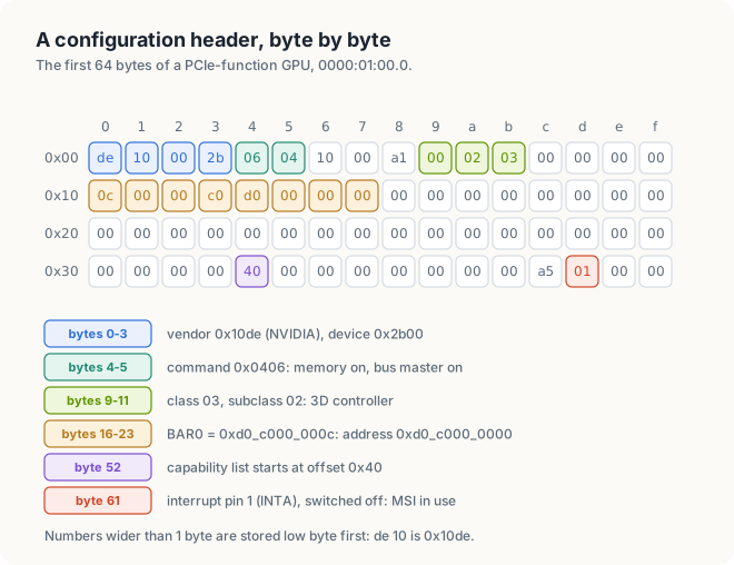
The header contains 6 fields of 4 bytes, at bytes 16 to 39, that tell the operating system where the function’s own registers and memory may be reached.
Definition 26.2 Base address register. A base address register, or BAR, is one of the 6 fields of a configuration header that each describe 1 window of the function’s registers or memory. The function decides how large the window is and of what kind; the operating system decides where in the physical address space the window starts, by writing the start address into the BAR. A 64-bit address occupies 2 neighboring fields.
Example. The BAR0 of the PCIe-function GPU holds the start address 0xd0_c000_0000 of a window of 16 MiB, which contains the GPU’s registers.
Worked example: decoding the configuration header
- Vendor and device, bytes 0 to 3: 0x10de is NVIDIA’s vendor number, assigned by the
PCI-SIG, the industry group that maintains the PCI standards; 0x2b00 is the device number NVIDIA gave this GPU.
lspci -nnprinted the same pair as[10de:2b00]. - Command, bytes 4 and 5: 0x0406 = binary 0000 0100 0000 0110. Bit 1 lets the function answer memory transactions (its BARs are live). Bit 2 lets it start transactions of its own (it may read and write memory: DMA, section 26.5). Bit 10 switches off the old interrupt wire in favor of messages (section 26.7).
- Class, bytes 9 to 11: programming interface 0x00, subclass 0x02, class 0x03. Class 3 is “display controller” and subclass 2 is “3D controller”, a GPU with no display output.
- BAR0, bytes 16 to 23: the 8 bytes read low first are 0x0000_00d0_c000_000c. Its low 4 bits, 0xc = binary 1100, are flags: bit 0 = 0, a memory window; bits 2:1 = 10, a 64-bit address; bit 3 = 1, prefetchable. With the flags cleared, the window starts at 0xd0_c000_0000.
The address in a BAR is thus the result of a negotiation between the function, which fixes the
size and kind of the window, and the operating system, which fixes its place. lspci -v prints
the result of that negotiation:
$ lspci -vv -s 0000:01:00.0 # Jetson AGX Thor, as a normal user
0000:01:00.0 3D controller: NVIDIA Corporation Device 2b00 (rev a1)
Control: I/O- Mem+ BusMaster+ SpecCycle- MemWINV- VGASnoop- ParErr- Stepping- SERR- ...
Interrupt: pin A routed to IRQ 421
IOMMU group: 83
Region 0: Memory at d0c0000000 (64-bit, prefetchable) [size=16M]
Capabilities: <access denied>
Kernel driver in use: nvidia
Mem+ BusMaster+ are bits 1 and 2 of the command register, and Region 0 is BAR0 at the
address decoded above. IRQ 421 is the number under which Linux lists the function’s interrupt,
and the IOMMU group is explained in section 26.6. The capabilities are a list of optional
features of the function, kept in the configuration space after the header. They start at offset
0x40, lie beyond the first 64 bytes, and Linux shows them only to root.
26.2.2 BAR sizing
lspci reported [size=16M], although no field of the header holds a size. The size is found
by a procedure that the PCI specification defines.
Let us first work the procedure on a BAR of only 8 bits, which we invent for the purpose and which describes a window of 16 bytes. A window of 16 = 24 bytes must start at a multiple of 16, such as 0x30 or 0xA0, and every multiple of 16 has 0 in its low 4 bits. The device therefore stores only the high 4 bits of the address and wires the low 4 bits to 0: whatever software writes there, they read back as 0. Software writes all ones, 0xFF = binary 1111 1111, and reads back 0xF0 = binary 1111 0000. Inverting the bits gives 0x0F = 15, and adding 1 gives 16, the size of the window.
Key observation A window of \(2^k\) bytes starts at a multiple of \(2^k\), so the low \(k\) bits of its address are always 0, and the device need not store them. The number of low bits that stay 0 after software writes all ones reveals \(k\), and therefore the size.
A real BAR works in the same way. A device implements only the high bits of each BAR’s address: the bits below the window’s size are wired to 0, because a window of \(2^k\) bytes must start at a multiple of \(2^k\). Software writes all ones into the BAR and reads it back; the bits that stayed 0 reveal the size. The lowest 4 bits of a memory BAR hold flags instead of address bits, so the flags must be cleared before the bits are inverted. Figure 26.4 works the procedure for the NVMe drive of figure 26.1 and for the PCIe-function GPU.
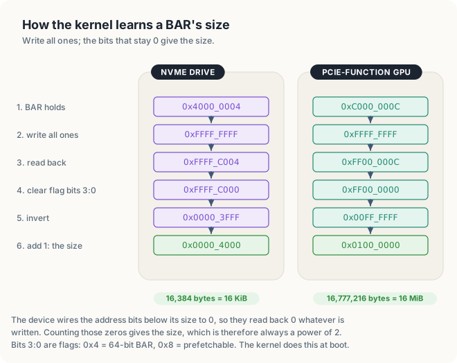
Let us follow the procedure for the NVMe drive. Its window is 16 KiB = 16,384 bytes =
\(2^{14}\) bytes, so address bits 13 to 0 of its BAR are wired to 0. When software writes
0xFFFF_FFFF, the low word reads back as 0xFFFF_C004: bits 31 to 14 are 1, bits 13 to 4 are 0,
and bits 3 to 0 hold the flags, 0x4, which mark a 64-bit memory window. Clearing the flags gives
0xFFFF_C000, inverting gives 0x0000_3FFF = 16,383, and adding 1 gives 16,384 bytes. The same
steps on the PCIe-function GPU give 0x0100_0000 = 16,777,216 bytes, the [size=16M] that
lspci printed.
The kernel performs this sizing once, at boot, for every BAR of every function. Ordinary programs never do it, and should not: a BAR full of ones points the device at the wrong address until it is restored. It follows from the procedure that the size of a BAR is always a power of 2. A GPU with 24 GiB of memory that wants all of it visible through 1 window needs a BAR of 32 GiB, the next power of 2.
26.2.3 Bus addresses and CPU addresses
The address written in a BAR is the address that the device sees on its link, a bus address. The CPU need not use the same number: the address with which the CPU reaches the window, the CPU address, may differ from the bus address by a fixed amount that the root port adds or subtracts. The NVMe drive of figure 26.1 shows the difference:
$ xxd -g1 -s 16 -l 8 /sys/bus/pci/devices/0004:01:00.0/config
00000010: 04 00 00 40 00 00 00 00 ...@....
$ lspci -v -s 0004:01:00.0 | grep Region
Region 0: Memory at 2428000000 (64-bit, non-prefetchable) [size=16K]
The BAR holds 0x4000_0000 (flags 0x4, a 64-bit window that is not prefetchable). The CPU
reaches the same registers at 0x24_2800_0000. The root port translates between the 2: a CPU
store to 0x24_2800_0000 + \(r\) leaves the root port as a PCIe write to bus address
0x4000_0000 + \(r\). For the PCIe-function GPU the 2 numbers happen to be equal: its BAR
holds 0xd0_c000_0000, and lspci reports the CPU address d0c0000000. A driver must never
assume either case; Linux keeps the two kinds of address apart in its types for exactly this
reason.
26.2.4 The BARs of a GPU
NVIDIA’s open-source kernel driver describes the windows of its GPUs. BAR0 holds the GPU’s registers. BAR1 is a window onto the GPU’s own memory, through which the CPU can read and write device memory with loads and stores. On consumer cards BAR1 has traditionally been 256 MiB, a small sliding view of the whole memory. With Resizable BAR, a PCIe feature that lets the system grow a BAR at boot, it can cover all of the memory. Data-center GPUs such as the A100 and the H100 offer a BAR1 at least as large as their memory.
The PCIe-function GPU has only BAR0, 16 MiB of registers. It has no memory of its own to
expose: its memory is the system’s DRAM, which the CPU already reaches directly. The device
tree of the platform-device GPU gives it a bar0 and a bar1 of 16 MiB each, plus a 4 KiB
window, again with no window onto a separate memory.
26.3 Memory-mapped I/O as the control path
26.3.1 Loads and stores with side effects
A load from DRAM has no effect on the memory, and reading the same address twice gives the same value. A load from a device register can have an effect: reading a status register may clear the event it reports, and 2 reads may return 2 different values because the device changed state in between. A store to a register is a command, such as “start”, “reset” or “new work is waiting”. Such effects are called side effects, and they change what the processor may do with the addresses.
Consider a status register that holds 1 when a copy has finished and that clears itself to 0 when it is read. The device finishes a copy, and the register holds 1. The driver loads it and gets 1. A second load gets 0, because the first load cleared it; the device reports each event exactly once. Now suppose that the processor kept a copy of the register in its cache, as it does for memory. The second load would be served from the cache and return 1 again, and the driver would count 1 finished copy twice. Suppose instead that the processor loaded the register early, on a guess that the program would soon need it, and then discarded the value. The register would be cleared, and the driver would never see the event at all.
A processor keeps copies of memory in its caches, small fast memories near the core, and it performs speculative reads: loads issued ahead of a program, on a guess that the program will need the data soon. Both behaviors are wrong for a device, as the example shows: a cached copy of a status register goes stale, and a load that the processor issued early may trigger a side effect the program never asked for. Every page in a program’s address space therefore carries a memory type in its page-table entry, the record of the page table that holds the page’s translation, and the memory type tells the processor how it may treat the addresses. Arm and x86 use different names for the types, and the table gives both:
| Memory type (Arm name; x86 name) | Cached | Speculative reads | Stores merged | Used for |
|---|---|---|---|---|
| Normal, cacheable (WB) | yes | yes | yes | DRAM |
| Normal, non-cacheable (WC, write-combining) | no | yes | yes | frame buffers, BAR1-like windows |
| Device-nGnRE (UC, uncached) | no | no | no | registers in BAR0 |
WB stands for write-back, the ordinary cached type; UC for uncached. In the Arm name Device-nGnRE, the letters state that the processor may not gather (nG) or reorder (nR) the accesses, and that a write may be acknowledged early (E), before it reaches the device. A frame buffer is the memory that holds the image shown on a display.
Write-combining memory is not cached, but the processor may gather several stores to neighboring addresses in a small buffer and send them as 1 larger transaction. For example, 16 stores of 4 bytes to the addresses 0x1000, 0x1004, …, 0x103C fill 64 neighboring bytes. Without combining they leave the core as 16 transactions of 4 bytes; with combining they leave as 1 transaction of 64 bytes. A program that fills a frame buffer or a command buffer with a stream of stores runs much faster that way. Device memory forbids even that. Each store reaches the device as written, in program order.
On PCIe the two directions differ in cost. A memory write is posted: the root complex sends it and lets the CPU continue at once, without waiting for any reply. A memory read is non-posted: it must wait for the device’s completion to travel back across the link, typically several hundred nanoseconds to more than a microsecond, a few thousand CPU cycles. Drivers therefore write registers freely and read them as rarely as they can.
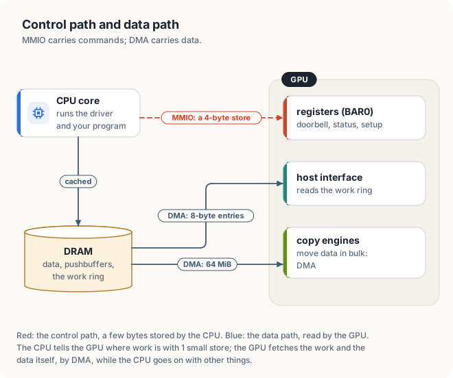
The CPU uses MMIO for control: a few bytes that tell the device what to do. Bulk data takes another path, in which the device itself reads and writes memory while the CPU does other work.
Definition 26.3 Direct memory access. Direct memory access, or DMA, is a transfer that a device performs itself, reading or writing memory without a CPU core moving each byte. The path of MMIO stores from the CPU to the device is the control path; the path of DMA between memory and the device is the data path.
Example. To copy 64 MiB to the GPU, the CPU writes a short description of the copy into memory and stores 4 bytes into a GPU register by MMIO. The GPU then reads the description, and the 64 MiB, from DRAM by DMA (figure 26.5).
26.3.2 CPU access speed by memory type
The registers of a GPU are out of reach of an ordinary program, but the memory types
are not. CUDA can allocate host memory with the write-combining type: cudaHostAlloc with the
flag cudaHostAllocWriteCombined. The second part of the chapter’s program runs the same 2
loops, a write of every word and a sum of every word, over 64 MiB of 4 kinds of memory: pageable
memory from malloc, which the operating system may move; pinned memory from cudaMallocHost;
pinned write-combined memory; and managed memory from cudaMallocManaged, which CPU and GPU
reach through the same pointer (Chapter 4).
Listing 26.2 The same CPU loops over each kind of memory.
fn main() -> Result<(), DriverError> {
// ...
let words = 16 << 20; // 16,777,216 words, 64 MiB
let mut pageable = vec![0u32; words];
let mut pinned = PinnedHostBuffer::<u32>::zeroed(&ctx, words)?;
println!("CPU access to 64 MiB through each mapping:");
time_cpu("Vec (pageable)", &mut pageable);
time_cpu("PinnedHostBuffer", pinned.as_mut_slice());
// ...
}// 2. The same CPU loops over 4 kinds of memory.
void memoryTypes()
{
const size_t bytes = 64u << 20;
const int reps = 5;
uint32_t* pageable = static_cast<uint32_t*>(std::malloc(bytes));
uint32_t* pinned = nullptr;
uint32_t* combined = nullptr;
uint32_t* managed = nullptr;
check(cudaMallocHost(&pinned, bytes));
check(cudaHostAlloc(&combined, bytes, cudaHostAllocWriteCombined));
check(cudaMallocManaged(&managed, bytes));
std::printf("CPU access to %zu MiB through each mapping:\n", bytes >> 20);
timeCpu("malloc (pageable)", pageable, bytes, reps);
timeCpu("cudaMallocHost (pinned)", pinned, bytes, reps);
timeCpu("write-combined pinned", combined, bytes, reps);
timeCpu("cudaMallocManaged", managed, bytes, reps);
std::printf("\n");
check(cudaFree(managed));
check(cudaFreeHost(combined));
check(cudaFreeHost(pinned));
std::free(pageable);
}
timeCpu writes the value 1 into every word, sums every word, keeps the best of 5 passes, and
checks that the sum equals the number of words. The output on both machines:
CPU access to 64 MiB through each mapping: # Orin NX
malloc (pageable) write 27.02 GB/s read 12.03 GB/s PASSED
cudaMallocHost (pinned) write 26.62 GB/s read 11.93 GB/s PASSED
write-combined pinned write 13.75 GB/s read 1.09 GB/s PASSED
cudaMallocManaged write 27.20 GB/s read 12.13 GB/s PASSED
CPU access to 64 MiB through each mapping: # Thor
malloc (pageable) write 41.61 GB/s read 20.52 GB/s PASSED
cudaMallocHost (pinned) write 41.43 GB/s read 20.61 GB/s PASSED
write-combined pinned write 41.44 GB/s read 20.69 GB/s PASSED
cudaMallocManaged write 41.38 GB/s read 20.69 GB/s PASSED
On the platform-device machine, 3 of the 4 kinds of memory behave alike, because all 3 are
ordinary cacheable DRAM to the CPU. They ran at about 27 GB/s for writes and 12 GB/s for reads,
the speed of 1 CPU core. Write-combined memory is different. Its reads ran at 1.09 GB/s, 12.03
/ 1.09 ≈ 11 times slower, because no read is served from a cache and none is fetched ahead:
each load waits for DRAM. Its writes ran at 13.75 GB/s, half the cached speed but 13 times its
own reads, because the write-combining buffer still merges the stores into whole lines. On the
PCIe-function machine the flag changed nothing: all 4 kinds ran at about 41 GB/s and 21 GB/s.
CUDA’s documentation describes the flag as a request that helps “on some system
configurations”, and there the memory was mapped cacheable. The Rust program measures the 2
kinds that cuda-core can allocate, Vec and PinnedHostBuffer; cuda-core has no
write-combined allocation at revision b7fe543 of its source. On the platform-device machine it found the same as
C++: 27.41 and 27.58 GB/s for writes, 12.43 and 12.32 GB/s for reads. Runs differ by about 10%
from one to the next.
26.3.3 Ordering writes before a doorbell
A device usually learns of new work in 2 steps. The CPU first writes the work itself into memory, then stores into 1 register, the doorbell, to tell the device to look. The order of those 2 steps decides whether the device sees the work. If the doorbell’s store reached the device first, the device would read the memory before the work was in it.
Let us follow 1 submission with numbers. Slot 3 of an array in memory holds 0, left over from earlier, and the CPU wants the device to run the command 42. It performs 2 stores:
store 1: slot[3] ← 42 (to cacheable memory)
store 2: doorbell ← 3 (to a device register: "slot 3 is ready")
If store 1 becomes visible first, the device receives the doorbell, reads slot 3 and finds 42. If store 2 becomes visible first, the device reads slot 3 before 42 has arrived and finds 0, the old value. The program is the same in both cases; only the order in which the 2 stores became visible differs.
The processor does not keep stores in program order on its own. An Arm core may let a later
store become visible before an earlier one, and stores to cacheable memory and stores to device
registers travel by different paths. A memory barrier is an instruction that keeps the order:
every memory access before it completes, as seen by other observers, before any after it. A memory
barrier differs from the barrier __syncthreads() of earlier chapters, which makes the threads of
a block wait for each other; a memory barrier orders the accesses of 1 thread. In this chapter,
“barrier” means a memory barrier. On Arm the barriers are the DMB and DSB instructions. In C++
and Rust, a store with release ordering is a store that becomes visible only after every
access that precedes it in the program; it places the barrier before the store. Linux’s writel(), the function a driver uses to
write a 32-bit register, puts a write barrier before the store for exactly this case, so that a
device started by the register sees every earlier write to memory. In Section 26.4.6, we show what
happens when the order is wrong.
Rule Write the work into memory, then execute a memory barrier, then store to the doorbell.
26.4 Work rings and doorbells
26.4.1 A ring of work entries
A kernel launch returns in microseconds because the CPU does not hand the work to the GPU and wait; it leaves the work in memory for the GPU to collect. Suppose that a program launches 3 kernels, A, B and C, in a row, and that each takes 1 ms on the GPU. If each launch waited for the GPU to accept the kernel, the CPU would wait for A to finish before it could hand over B. If the CPU instead writes A, B and C into a list in memory, 1 after another, it can return from the 3 launches at once, and the GPU takes the kernels from the list in order. The list needs a fixed size, because memory for it is set aside in advance, and it must be reusable, because a program may launch millions of kernels. Both needs are met by using a fixed array in a circle.
Definition 26.4 Ring buffer, PUT and GET. A ring buffer is an array of a fixed number \(n\) of slots, used in a circle, with 2 counters. PUT counts the entries the producer, here the CPU, has written, and GET counts the entries the consumer, here the GPU, has finished. Both only grow. Entry number \(c\) lives in slot \(c \bmod n\), the remainder of \(c\) divided by \(n\), so the slots are reused once the ring wraps around.
Example. With \(n\) = 8 slots, entry #9 lives in slot 9 mod 8 = 1, the slot that entry #1 used before it.
The entries waiting to be run are those from GET to PUT − 1, so there are PUT − GET of them. The ring is empty when PUT = GET and full when PUT − GET = \(n\). The pseudocode shows both sides.
host, to submit entry e: device, forever:
while PUT - GET = n: wait wait until GET ≠ PUT
ring[PUT mod n] ← e run ring[GET mod n]
barrier GET ← GET + 1
PUT ← PUT + 1 (the doorbell)
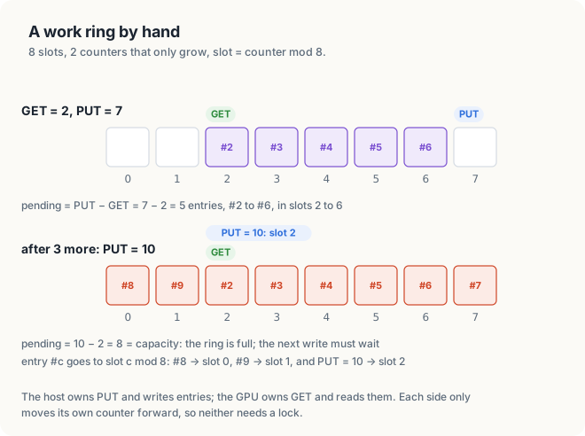
Worked example: a ring of 8 slots
- GET = 2 and PUT = 7: entries #2 to #6 are waiting, PUT − GET = 7 − 2 = 5 of them, in slots 2 to 6.
- The host writes 3 more entries. Entry #7 goes to slot 7 mod 8 = 7, #8 to slot 8 mod 8 = 0, #9 to slot 9 mod 8 = 1. PUT is now 10.
- PUT − GET = 10 − 2 = 8 = the number of slots: the ring is full. Entry #10 would go to slot 10 mod 8 = 2, which still holds #2, not yet run; the host must wait until GET passes 2.
- Each counter has 1 writer: the host moves PUT, the device moves GET. Neither side needs a lock, a variable that lets only 1 thread at a time into a section of code.
| Symbol | Meaning | In the example |
|---|---|---|
| \(n\) | number of slots in the ring | 8 |
| PUT | entries written by the host so far | 7, then 10 |
| GET | entries finished by the device so far | 2 |
| PUT − GET | entries waiting; the ring is full when it equals \(n\) | 5, then 8 |
| \(c \bmod n\) | slot of entry \(c\) | #9 → slot 1 |
26.4.2 The ring and the doorbell of an NVIDIA GPU
An NVIDIA GPU receives work through channels. A channel is 1 ordered stream of commands from 1 process, a running program with its own address space, to the GPU; the CUDA runtime places each stream’s work on 1 of a pool of channels. Each channel has 3 structures in memory that both the CPU and the GPU can reach. NVIDIA’s open-source kernel driver publishes their layouts in its class headers, C header files that define the registers and memory structures of each generation of GPU:
- The pushbuffer holds the commands themselves, called methods: “set this kernel’s parameters”, “launch with this grid”, “signal this semaphore”. A semaphore here is a word in memory that the GPU writes when it reaches a point in the stream of commands, so that the CPU can learn how far the GPU has come. A launch is a short run of methods.
- The GPFIFO is the ring of the previous section. Each entry is 8 bytes and points at a
piece of the pushbuffer: its address and its length (
GP_ENTRY__SIZE= 8 in the headers). - USERD is a small page of counters for the channel. At offset 0x8c it holds
GPPut, the ring’s PUT, which the CPU writes; at offset 0x88,GPGet, which the GPU writes.
Since the Volta generation of 2017, the doorbell is a register named NOTIFY_CHANNEL_PENDING, at
offset 0x90 of a 64 KiB “user mode” window that the headers place at offset 0x81_0000 of BAR0.
The CPU stores the channel’s work-submit token, a number the driver gives each channel,
into that register. A system call is a request from a program to the operating-system kernel,
in which the processor switches into the kernel and back; it costs far more than a store. The
register’s page is mapped into the process, that is, the process’s page table holds an entry
for it, so the process can store to the register directly and needs no system call. Figure 26.7
puts the steps of 1 launch in order.
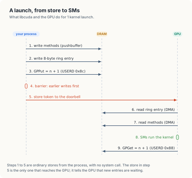
Steps 1 to 5 are the launch call that we timed in Chapter 6: a few ordinary stores into memory, 1 barrier and 1 store to a register, 3.77 µs with the rest of the runtime’s work. Steps 6 to 9 happen later, on the GPU’s own time. The part of the GPU that reads the ring, its host interface, fetches entries and methods from memory by DMA, so the CPU never waits for the GPU to accept anything. Only when the ring is full does a launch wait, exactly as the host waits in the worked example.
26.4.3 Doorbells in an NVMe drive
The design is not peculiar to GPUs. An NVMe drive, whose specification is public, takes its commands the same way. The host writes 64-byte commands into a submission queue in memory, then writes the queue’s new tail, the slot after the last command written, which plays the role of PUT, into a doorbell register in BAR0. The drive reports finished commands in a second ring, the completion queue, and the host tells the drive how far it has read that ring by writing the queue’s head, the role of GET, into a second doorbell. The drive has 1 pair of queues for administration commands, such as creating queues, and further pairs for I/O queues, which carry reads and writes of data. The specification places the doorbells right after the drive’s 4 KiB of control registers. In the formulas, \(a \ll b\) means \(a\) shifted left by \(b\) bits, which is \(a \times 2^b\):
\[ \text{SQ tail doorbell of queue } y = \text{0x1000} + 2y \cdot (4 \ll \text{DSTRD}) \]
\[ \text{CQ head doorbell of queue } y = \text{0x1000} + (2y + 1) \cdot (4 \ll \text{DSTRD}) \]
| Symbol | Meaning | On the drive of figure 26.1 |
|---|---|---|
| \(y\) | queue number; 0 is the administration queue | 0 to 8 |
| DSTRD | doorbell stride, read from the drive’s capability register | 0 (the usual value) |
| \(4 \ll \text{DSTRD}\) | bytes between doorbells | 4 |
Before we use the formulas on the real drive, let us place the doorbells of the first 2 queues by hand, with DSTRD = 0 and so 4 bytes between doorbells. Queue 0 has its submission doorbell at 0x1000 + 0 × 4 = 0x1000 and its completion doorbell at 0x1000 + 1 × 4 = 0x1004. Queue 1 follows at 0x1000 + 2 × 4 = 0x1008 and 0x1000 + 3 × 4 = 0x100C. The doorbells thus alternate, submission and completion, queue after queue, each 4 bytes wide.
For example, /proc/interrupts, a file in which Linux lists every interrupt line and the number
of interrupts each has received, lists 9 interrupt lines for the drive of figure 26.1,
nvme0q0 to nvme0q8: the administration queue and 8 I/O queues, 1 per CPU core. With a
stride of 4 bytes, the submission doorbell of queue 8 sits at 0x1000 + 2 × 8 × 4 = 0x1040, and
its completion doorbell at 0x1000 + 17 × 4 = 0x1044. The highest doorbell, at 0x1047, lies well
inside the 16 KiB = 0x4000-byte BAR0 that we sized in figure 26.4.
26.4.4 A software model of a work ring
The chapter’s program builds the mechanism with 2 CPU threads, so that we can run it, time it, and observe what happens when the order of writes is wrong. A host thread submits entries; a device thread plays the GPU’s host interface. Each entry carries an opcode, a number that names the operation requested, and an argument. The device thread spends 2 µs on each entry, a stand-in for a kernel, and adds the argument to a sum, so the program can check that every entry was run exactly once.
The doorbell here is an atomic counter, PUT, that the device thread watches. An atomic variable is one whose loads and stores another thread never sees half done, and whose accesses can carry an ordering such as release. A real device would be woken by a store to its register instead of watching memory, but the order of events is the same. A cache line is the unit of 64 bytes in which the CPU’s caches hold and move memory. Each counter sits on its own cache line, as each register of a device has its own address.
Listing 26.3 The ring, the device and the doorbell.
const CAPACITY: u32 = 64;
/// Keeps 1 value alone on a 64-byte cache line, as each register has its own address.
#[repr(align(64))]
struct Line<T>(T);
/// A ring of entries (opcode in the high 32 bits, argument in the low 32) and 2 counters.
struct Channel {
ring: [AtomicU64; CAPACITY as usize],
doorbell: Line<AtomicU32>, // PUT: entries written so far
get: Line<AtomicU32>, // GET: entries the device has finished
stop: Line<AtomicBool>,
}
/// The device: wait for the doorbell, run every entry up to PUT, then report GET.
fn device(ch: &Channel, work_us: f64) -> u64 {
let mut get = 0u32;
let mut sum = 0u64;
while !ch.stop.0.load(Ordering::Acquire) {
let put = ch.doorbell.0.load(Ordering::Acquire);
while get != put {
let entry = ch.ring[(get % CAPACITY) as usize].load(Ordering::Relaxed);
spin_us(work_us);
sum += if entry >> 32 == 1 { entry & 0xffff_ffff } else { 0 };
get += 1;
ch.get.0.store(get, Ordering::Release);
}
}
sum
}
/// The host: write the entry, then ring the doorbell. Waits only when the ring is full.
fn submit(ch: &Channel, depth: u32, put: &mut u32, arg: u32) {
while put.wrapping_sub(ch.get.0.load(Ordering::Acquire)) >= depth {
spin_loop();
}
let entry = (1u64 << 32) | arg as u64;
ch.ring[(*put % CAPACITY) as usize].store(entry, Ordering::Relaxed);
ch.doorbell.0.store(*put + 1, Ordering::Release);
*put += 1;
}// 3. A ring of work entries and a doorbell, between a host thread and a device thread.
struct Entry {
uint32_t opcode;
uint32_t arg;
};
struct Channel {
static const uint32_t capacity = 64;
Entry ring[capacity];
// Each counter on its own 64-byte cache line, as each register has its own address.
alignas(64) std::atomic<uint32_t> doorbell{0}; // PUT: entries written so far
alignas(64) std::atomic<uint32_t> get{0}; // GET: entries the device finished
alignas(64) std::atomic<bool> stop{false};
uint64_t sum = 0; // the device's result
};
// The device: wait for the doorbell, run every entry up to PUT, then report GET.
void device(Channel* ch, double workUs)
{
uint32_t get = 0;
while (!ch->stop.load(std::memory_order_acquire)) {
uint32_t put = ch->doorbell.load(std::memory_order_acquire);
while (get != put) {
Entry e = ch->ring[get % Channel::capacity];
spinUs(workUs);
ch->sum += e.opcode == 1 ? e.arg : 0;
get += 1;
ch->get.store(get, std::memory_order_release);
}
}
}
// The host: write an entry, then ring the doorbell. Waits only when the ring is full.
void submit(Channel* ch, uint32_t depth, uint32_t& put, uint32_t arg, bool doorbellFirst)
{
while (put - ch->get.load(std::memory_order_acquire) >= depth) {
}
Entry& slot = ch->ring[put % Channel::capacity];
if (doorbellFirst) {
ch->doorbell.store(put + 1, std::memory_order_release);
slot = Entry{1, arg};
} else {
slot = Entry{1, arg};
ch->doorbell.store(put + 1, std::memory_order_release);
}
put += 1;
}
submit waits while the ring holds depth entries, writes the entry, then stores PUT + 1 with
release ordering: the barrier of section 26.3.3, built into the store. The device loads PUT
with acquire ordering, the counterpart of release. No access that follows the load in the
program may become visible before it. The 2 orderings pair: once the device sees PUT = \(c\) +
1, it also sees entry \(c\). The doorbellFirst branch exists to break that order on purpose
(section 26.4.6).
Rust’s version stores each entry in an AtomicU64, with the opcode in the high 32 bits. Rust
does not allow 2 threads to touch the same plain memory when one of them writes, so the slots are
atomics too. A Relaxed store is an atomic store that promises no ordering with other accesses;
it compiles to an ordinary store, and the Release store of the doorbell provides the order.
26.4.5 Ring depth and run-ahead
The program submits 200 bursts of 32 entries. After each burst the host does 64 µs of work of its own, so the work a GPU would do and the work the CPU does could overlap. A burst is a group of entries that the host submits one after another without other work in between. The depth of a ring is its number of slots \(n\), and it limits the run-ahead of the host: the number of entries by which the host may be ahead of the device. We run the program with a ring of depth 1, 4, 32 and 64: the host may run at most that many entries ahead of the device. Before we run it, we can predict the time of 1 burst.
Worked example: 1 burst at depth 1, 4 and 32
- The device needs 32 entries × 2 µs = 64 µs per burst, and the host needs 64 µs for its own work.
- Depth 1: the host can submit entry \(k\) only after the device has finished entry \(k − 1\). It waits through almost all 64 µs of the device’s work, then works alone for 64 µs. A burst takes about 64 + 64 = 128 µs, and 200 bursts take 200 × 128 µs = 25.6 ms.
- Depth 4: the host writes 4 entries at once, then 1 more each time the device finishes 1. Its last entry goes in after the device has finished 28: 28 × 2 µs = 56 µs. Then come 64 µs of its own work: 56 + 64 = 120 µs per burst, 200 × 120 µs = 24.0 ms.
- Depth 32: the whole burst fits. The host writes 32 entries in about a microsecond and starts its own work while the device runs them; both take 64 µs, so a burst takes 64 µs, and 200 bursts take 12.8 ms. Depth 64 can do no better.
Work queue: 200 bursts of 32 entries, 2 us each, 64 us of host work: # Orin NX, C++
depth 1, entry first 30.85 ms sum 20483200 of 20483200 PASSED
depth 4, entry first 26.01 ms sum 20483200 of 20483200 PASSED
depth 32, entry first 13.69 ms sum 20483200 of 20483200 PASSED
depth 64, entry first 14.21 ms sum 20483200 of 20483200 PASSED
Work queue: 200 bursts of 32 entries, 2 us each, 64 us of host work: # Thor, C++
depth 1, entry first 28.66 ms sum 20483200 of 20483200 PASSED
depth 4, entry first 25.76 ms sum 20483200 of 20483200 PASSED
depth 32, entry first 13.50 ms sum 20483200 of 20483200 PASSED
depth 64, entry first 13.49 ms sum 20483200 of 20483200 PASSED
Work queue: 200 bursts of 32 entries, 2 us each, 64 us of host work: # Orin NX, Rust
depth 1 29.80 ms sum 20483200 of 20483200 PASSED
depth 4 25.01 ms sum 20483200 of 20483200 PASSED
depth 32 13.69 ms sum 20483200 of 20483200 PASSED
depth 64 13.86 ms sum 20483200 of 20483200 PASSED
Every run summed all 6,400 arguments, 1 + 2 + … + 6,400 = 6,400 × 6,401 / 2 = 20,483,200, so every entry ran exactly once. The times follow the prediction. Depth 1 took 28.7 to 30.9 ms against 25.6 ms predicted, depth 4 took 25.0 to 26.0 ms against 24.0 ms, and depths 32 and 64 took 13.5 to 14.2 ms against 12.8 ms. The measured times sit 4% to 21% above the predictions: the cost of the threads waking, the clock reads and the cache lines moving between the 2 cores. Figure 26.8 draws 1 burst at depth 1 and at depth 32.
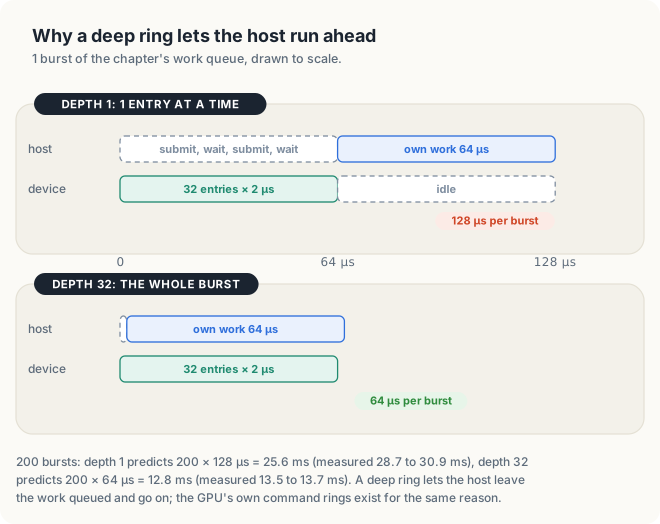
Key observation The host’s own work overlaps the device’s work only for the entries that the ring can hold. When the ring holds the whole burst, the host submits everything at once, and the two kinds of work run side by side.
Note that the ring halves the total time only when it holds the whole burst. A ring is a queue, and a queue lets the producer run ahead of the consumer by as many entries as it holds; this is the mechanism behind Chapter 6’s asynchronous launches and streams. A GPU’s rings hold hundreds of entries, so a program can queue many kernels and copies before it must wait.
A launch is a few stores into a ring in memory and 1 store to a doorbell. The deeper the ring, the further the CPU can run ahead of the GPU.
26.4.6 Ordering errors
Run with --doorbell-first, the program stores PUT + 1 before it writes the entry. The device
may then see the new PUT, read the slot, and find whatever the slot held before: an entry from
the previous lap, the previous pass of the counters around the ring, or nothing. For example,
in a ring of 8 slots, entry #9 goes to slot 1, which still holds entry #1. If the device reads
slot 1 between the doorbell and the write of entry #9, it runs the argument of entry #1 a second
time and never runs that of entry #9.
$ ./systems --doorbell-first # Orin NX
depth 1, doorbell first 31.50 ms sum 20479232 of 20483200 FAILED
depth 4, doorbell first 25.35 ms sum 20483200 of 20483200 PASSED
depth 32, doorbell first 13.50 ms sum 20483200 of 20483200 PASSED
depth 64, doorbell first 13.50 ms sum 20483200 of 20483200 PASSED
At depth 1 the device read stale slots and lost 20,483,200 − 20,479,232 = 3,968 from the sum. The other 3 depths passed in this run. Over 5 runs on the platform-device machine, 4 of the 20 results were wrong, and on the PCIe-function machine 3 of 12; which ones fail changes from run to run. Depth 1 fails most often, because the device thread is idle and watching PUT when the doorbell rings, so it reaches the slot in the instant before the entry arrives. The same swap in the Rust program failed at depth 1 in all 5 runs.
The Rust version shows a further point. A data race is a pair of accesses to the same plain, non-atomic memory by 2 threads, at least one of them a write, with nothing that orders them. Rust does not compile a program in which 2 threads touch the same plain memory in this way, so the slots had to be atomics. The broken program is nevertheless free of data races in Rust’s sense, and it still loses entries. The compiler can prove that every access is safe, but not that the protocol, entry first and doorbell second, is followed. The C++ version is worse off. There the swap also creates a data race, and its behavior is undefined: the language does not specify what the program does. In a driver, the same mistake causes the GPU to execute stale commands, rarely and usually under load.
Write the work, then a barrier, then the doorbell. In the other order, the program passed most runs and failed some, which makes the error hard to find.
26.5 DMA as the data path
Recall from Definition 26.3 that DMA is a transfer that a device performs itself, reading or
writing memory without a CPU core moving each byte. A PCIe function may do it only while its bus
master bit is set, bit 2 of the command register that figure 26.3 decoded (BusMaster+ in
lspci). A GPU uses DMA for 2 different jobs. Its host interface reads the work rings and
pushbuffers, as in steps 6 and 7 of figure 26.7. Its copy engines, units that do nothing
but move data, carry out cudaMemcpy and its asynchronous forms; both GPUs of listing 26.1
report 2 of them.
A copy engine is told what to move by a descriptor, a small record in memory with a source
address, a destination address and a length. A copy of 64 MiB from a host buffer to a device
buffer, for example, can be described by 1 descriptor that holds the address of the host buffer,
the address of the device buffer and the length 67,108,864 bytes. For cudaMemcpy from a host
buffer to the device, the sequence is:
- The driver makes sure the host buffer’s pages cannot move, by pinning them or by staging the data through a pinned buffer, that is, by copying it first into a pinned buffer of its own (section 4.2.2 explains why).
- It writes one or more descriptors, as methods in a channel’s pushbuffer.
- It rings the channel’s doorbell, as in section 26.4.2.
- The copy engine reads the descriptors, then reads the source by DMA and writes the destination, while the CPU does other work.
- The engine signals completion, by writing a value into memory that the driver checks or by raising an interrupt (section 26.7).
The addresses in a descriptor are the addresses that the device uses, not the CPU’s virtual addresses. On a system with an IOMMU they are not physical addresses either, as the next section explains.
26.6 The IOMMU
A device that can write any physical address can overwrite any memory, including the kernel’s. A faulty device, or a malicious one plugged into an external port, could then take over the machine. The remedy is the same as for processes: give the device addresses of its own, and translate them through a table that only the kernel can change.
Let us follow 1 translation by hand, with the example addresses of figure 26.9. A device is given a buffer of 4 pages of 4 KiB that it sees at the device addresses 0x1000_0000 to 0x1000_3FFF. In physical memory, the 4 pages lie scattered, at the physical pages that the figure numbers 3, 0, 5 and 1. The device writes to the address 0x1000_2010. The translation takes 3 steps:
- Subtract the start of the buffer: 0x1000_2010 − 0x1000_0000 = 0x2010.
- Split the result into a page number and an offset: 0x2010 / 0x1000 = page 2, remainder 0x010.
- Look up page 2 in the table, which gives physical page 5, and add the offset: the write lands at byte 0x010 of physical page 5.
A write to the address 0x2000_0000 finds no entry in the table. The translation fails, the write is refused, and the memory that the address would have reached is untouched.
Definition 26.5 IOMMU. An IOMMU (input-output memory management unit; the Arm name is SMMU, system MMU) sits between devices and memory and does for DMA what the CPU’s MMU does for loads and stores. It translates every address a device uses, an I/O virtual address or IOVA, through page tables that the kernel controls, and it refuses any address the kernel has not mapped for that device.
Example. In figure 26.9, the IOVA 0x1000_2010 is translated to byte 0x010 of physical page 5, and the IOVA 0x2000_0000 is refused with a fault, an error that the IOMMU reports to the kernel.
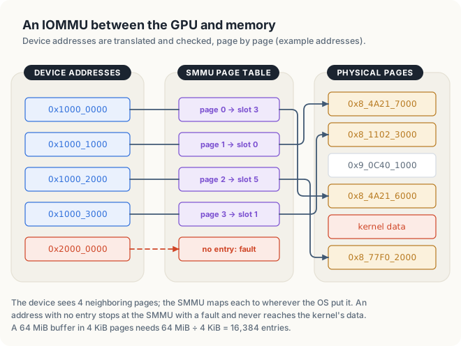
The IOMMU gives 2 benefits besides safety. A buffer whose pages lie scattered in physical memory looks contiguous, a single unbroken range of addresses, to the device, so 1 descriptor can cover it. And the kernel can take a mapping away, for example when a device is unplugged or handed to a virtual machine, a complete operating system that runs as a program on top of another.
The mappings have a cost. A 64 MiB buffer in 4 KiB pages has 67,108,864 ÷ 4,096 = 16,384 pages, so before a copy engine can read it, the kernel writes 16,384 entries into the IOMMU’s page table. The IOMMU caches recent translations in its own TLB (translation lookaside buffer), a small cache of page-table entries. A buffer that is pinned once and reused keeps its entries, whereas a buffer that is pinned again for every copy has them rebuilt each time; section 4.2.3 discusses why pinning is slow to set up.
Both machines route their devices through SMMUs. The platform-device machine has 3 SMMU
instances, separate SMMU units that each serve part of the devices, and 53 IOMMU groups,
sets of devices that the IOMMU cannot tell apart and that are always isolated together; its NVMe
drive is in group 5. The PCIe-function machine has 5
SMMU instances of Arm’s version 3 and 86 groups; its GPU is in group 83 (IOMMU group: 83 in
the lspci output of section 26.2.1).
Some systems let a device go further and use the CPU’s own page tables. With ATS, address
translation services, a PCIe device asks the IOMMU for translations and caches them, and the
IOMMU can walk, that is, read entry by entry, the same page tables the CPU uses for a
process. nvidia-smi -q on the
PCIe-function machine reports Addressing Mode : ATS. This is why its GPU printed
pageableAccess 1 and viaHostPageTables 1 in listing 26.1: it can follow a pointer returned
by malloc, because it translates the address the same way the CPU does. The platform-device
GPU printed 0 for both, so a kernel there needs memory that CUDA allocated or registered.
26.7 The kernel-mode and user-mode drivers
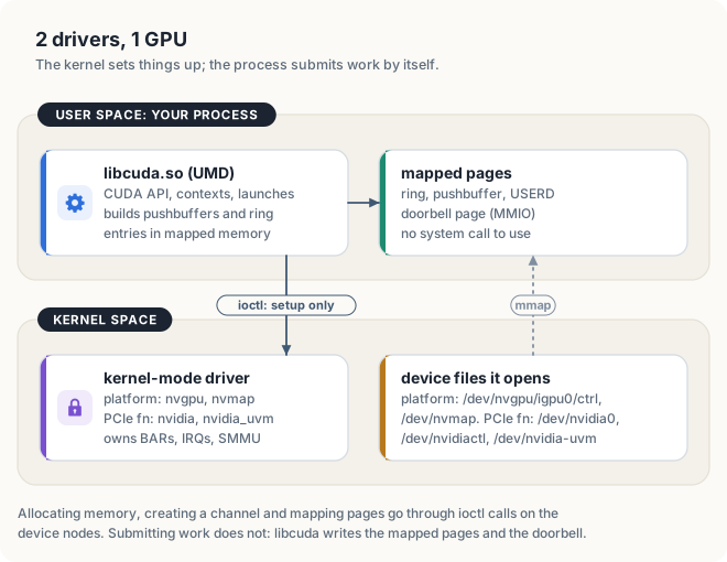
The GPU is driven by 2 pieces of software, and the division between them follows from the cost of entering the kernel. Consider a program that allocates 1 buffer and then launches 1,000 kernels. The allocation changes page tables and the IOMMU, which only the kernel may do, so it must enter the kernel, but it happens once. The 1,000 launches happen often, and each needs only the stores of section 26.4.2, which a process can make itself once the right pages are mapped into it. The work is therefore split: the rare work that needs privileges goes to a part of the driver inside the kernel, and the frequent work goes to a part inside the process.
Definition 26.6 Kernel-mode and user-mode drivers. The kernel-mode driver (KMD) is the part of the GPU driver that runs inside the operating-system kernel. It alone maps the GPU’s BARs, programs the IOMMU, handles the GPU’s interrupts, manages its power and clocks, and allocates its memory. The user-mode driver (UMD) is the part of the driver that is a library loaded into each process. It implements the API, builds pushbuffers and ring entries, and keeps each context’s state.
Example. For CUDA, the UMD is libcuda.so, the library behind both the runtime API and the
driver API. cudaMalloc asks the KMD for memory; a kernel launch is made by libcuda.so alone.
A CUDA context holds the state of 1 process on 1 GPU: its allocations, its loaded kernels and
its channels. A program reaches the KMD through device files, special files in /dev whose
operations the kernel forwards to a driver. The UMD opens them, calls ioctl on them to ask for
setup work (allocate memory, create a channel), and calls mmap on them to map pages into the
process. ioctl is the system call that sends a driver-specific request through an open device
file, and mmap is the system call that maps pages, here pages of a device file, into the
address space of the process. Among those pages are the channel’s ring, pushbuffer and USERD, and the page holding
the doorbell register. From then on the UMD submits work by itself, with ordinary stores
(figure 26.10).
The 2 machines use different KMDs, which the chapter’s program shows. Each KMD is a kernel
module, a piece of the kernel that is loaded separately, and Linux shows the files that a
process holds open under /proc/<pid>/fd, where <pid> is the number of the process. Listing
the device files that a running systems process holds open:
$ ls -l /proc/<pid>/fd | grep /dev # Orin NX: nvgpu and nvmap modules
/dev/nvgpu/igpu0/ctrl /dev/nvmap /dev/dri/render...
$ ls -l /proc/<pid>/fd | grep /dev # Thor: nvidia and nvidia_uvm modules
/dev/nvidia0 (18 times) /dev/nvidiactl /dev/nvidia-uvm (2 times) /dev/nvmap ...
On the PCIe-function machine the process also had 13 mappings of /dev/nvidiactl and 2 of
/dev/nvidia0 in its address space. The platform-device GPU is driven by nvgpu, NVIDIA’s
driver for Tegra GPUs, the GPUs built into NVIDIA’s Tegra and Jetson chips, which binds to the
platform device 17000000.gpu under the name gk20a. The PCIe-function GPU is driven by
nvidia, the same open kernel module that drives discrete GPUs, with nvidia_uvm for unified
memory, the managed memory of section 26.3.2.
The split explains three facts that we stated in earlier chapters without a reason. A launch costs a few microseconds, not the tens that a system call and a return would add, because it does not enter the kernel. A CUDA context belongs to a process, because the mappings and the channels belong to a process. And a crashed kernel ends with an error in 1 process, not a crashed machine, because the KMD stays in control of the GPU and can reset the faulty channel.
Interrupts go the other way, from the device to the CPU. A device raises one to report an event, such as a finished copy or a fault, and the CPU stops what it is doing to run the KMD’s handler, the routine of the driver that deals with the event. The interrupt controller is the unit that collects the interrupts of all devices and delivers them to the CPU cores. The platform-device GPU uses wires into the interrupt controller, named in its device tree; the PCIe-function GPU sends MSI (message-signaled interrupts), which are memory writes to a special address, so they need no wire.
The device tree of the platform-device GPU gives it 4 interrupts, numbered 0x44, 0x46, 0x47 and
0x43 among the interrupt controller’s shared peripheral interrupts, the interrupts of devices
that any core may handle, and named stall0, stall1, stall2 and nonstall. The Arm
interrupt controller is called the GIC, generic interrupt controller. On a GICv3, numbers 0 to
31 are reserved for interrupts that belong to 1 core, so shared peripheral interrupts start at
number 32, so 0x44 = 68 becomes interrupt 68 + 32 = 100, and
/proc/interrupts lists it as GICv3 100 gk20a_stall; the other 3 appear as 99, 102 and 103.
Line 103 had counted 49,415,447 interrupts after 2,590,200 s of uptime, the time since the
machine started, or about 19 interrupts per second. The PCIe-function GPU uses 8 MSI
vectors, separate MSI interrupts each with its own number, listed as 8 lines named
nvidia.
Interrupts are for events that the CPU must hear about. The submission of work never needs one: the doorbell is a store from the CPU, and the CPU learns that work has finished by reading GET, or a semaphore the GPU wrote, in memory.
26.8 Observing the system on Linux
The mechanisms of this chapter can be observed on any Linux machine with a GPU, without root
privileges. The table lists the commands and what each one showed on the 2 machines. The file
/proc/<pid>/maps lists every mapped range of a process’s address space, with the file, if any,
that each range maps, and /sys/class/iommu and /sys/kernel/iommu_groups list the IOMMU
instances and groups of section 26.6.
| Command | Shows | Platform-device GPU | PCIe-function GPU |
|---|---|---|---|
lspci -nn | PCIe functions with vendor and device | no GPU on PCIe | 01:00.0 [10de:2b00] |
lspci -vv -s <addr> | command bits, BARs, IOMMU group, driver | NVMe: 16K BAR0, group 5 | GPU: 16M BAR0, group 83, nvidia |
xxd -l 64 /sys/bus/pci/devices/<addr>/config | the configuration header | NVMe | GPU |
/sys/bus/platform/devices/*gpu* | platform devices and their driver | 17000000.gpu, gk20a | none |
/sys/firmware/devicetree/base/.../reg | register windows from the device tree | 3 windows | not needed |
/proc/interrupts | interrupt lines and counts | gk20a_stall on GIC 99 to 103 | 8 × nvidia (MSI) |
ls /sys/class/iommu, /sys/kernel/iommu_groups | IOMMU instances and groups | 3, 53 groups | 5 (SMMUv3), 86 groups |
/proc/<pid>/fd, /proc/<pid>/maps | device files a CUDA process uses | nvgpu/igpu0/ctrl, nvmap | nvidia0, nvidiactl, nvidia-uvm |
nvidia-smi -q | bus ID, addressing mode, BAR1 size | not available | ATS |
One file needs root: /proc/iomem, the kernel’s map of the physical address space. An ordinary
user sees its names but every address as 0, because physical addresses help an attacker who is
trying to exploit a kernel bug:
$ grep gpu /proc/iomem # Orin NX, as a normal user
00000000-00000000 : 17000000.gpu gpu@17000000
00000000-00000000 : 17000000.gpu gpu@17000000
The platform-device GPU is not in lspci. How does Linux find it, and where are its registers?
It is a platform device: the firmware’s device tree describes it, and Linux reads the
description at boot. Its reg property gives 3 windows: 16 MiB at 0x1700_0000, 16 MiB at
0x1800_0000 and 4 KiB at 0x03B4_1000. The gk20a driver, part of the nvgpu module, binds to
it.
26.9 CUDA calls and the mechanisms beneath them
We can now relate each CUDA call that touches the hardware to the mechanisms of this chapter. 4
terms in the table need a word of explanation. The GPU has its own page tables, so a pointer
returned by cudaMalloc is a GPU virtual address, which the GPU translates as the CPU’s MMU
translates a CPU virtual address. Zero-copy access is a kernel’s direct access to pinned host
memory through the bus, without a copy into device memory. A page fault is the event in which
a processor finds no valid translation for an address; managed memory uses it to migrate
pages, that is, to move them to the processor that touched them. Peer access is the access by
1 GPU to the memory of another GPU.
| CUDA call | What happens underneath |
|---|---|
cudaMalloc | the KMD allocates device memory and maps it in the GPU’s page tables; the pointer is a GPU virtual address |
kernel<<<...>>> | the UMD writes methods and a ring entry, then stores to the doorbell; no system call |
cudaMemcpy | pins or stages the host buffer, writes copy descriptors, rings the doorbell, waits for completion |
cudaMemcpyAsync | the same on a stream’s channel, without the wait, so copies overlap kernels (Chapter 6) |
cudaMallocHost | pins host pages and maps them in the IOMMU once, so copy engines can read them directly |
cudaHostAlloc(..., cudaHostAllocWriteCombined) | pinned memory mapped write-combining for the CPU: fast streaming writes, slow reads |
cudaHostGetDevicePointer | gives the GPU an address for pinned host memory (zero-copy, section 4.6) |
cudaMallocManaged | 1 address for CPU and GPU; pages migrate on faults, or are shared outright with ATS |
cudaDeviceEnablePeerAccess | lets 1 GPU’s DMA reach another GPU’s memory (Chapter 27) |
cudaStreamSynchronize | waits until the stream’s GET passes its last entry, by polling memory or by an interrupt |
26.10 The complete programs
Listing 26.4 The complete programs. code/oxide/ch17_systems/src/main.rs and code/ch17_systems/systems.cu
//! Chapter 17 in Rust: what the driver reports about the GPU, CPU access to pinned
//! memory, and a work queue with a doorbell between 2 threads.
//!
//! cargo oxide run
use std::hint::{black_box, spin_loop};
use std::sync::atomic::{AtomicBool, AtomicU32, AtomicU64, Ordering};
use std::thread;
use std::time::Instant;
use cuda_core::sys::CUdevice_attribute_enum_CU_DEVICE_ATTRIBUTE_INTEGRATED as INTEGRATED;
use cuda_core::sys::{CUdevice, CUdevice_attribute, cuDeviceGetAttribute};
use cuda_core::{CudaContext, DriverError, IntoResult, PinnedHostBuffer};
/// Asks the driver for 1 integer attribute of `device`.
fn attribute(device: CUdevice, which: CUdevice_attribute) -> Result<i32, DriverError> {
let mut value = 0;
// SAFETY: `value` is a valid place for 1 integer, and `device` came from a live context.
unsafe { cuDeviceGetAttribute(&mut value, which, device).result()? };
Ok(value)
}
/// Sums every word, so that the reads cannot be skipped.
fn cpu_read(x: &[u32]) -> u32 {
x.iter().fold(0u32, |s, &v| s.wrapping_add(v))
}
/// Best-of-5 CPU write and read bandwidth over `x`, in GB/s.
fn time_cpu(name: &str, x: &mut [u32]) {
let bytes = (x.len() * size_of::<u32>()) as f64;
let mut best_write = f64::MAX;
let mut best_read = f64::MAX;
let mut sum = 0;
for _ in 0..5 {
let t0 = Instant::now();
x.fill(1);
let t1 = Instant::now();
sum = black_box(cpu_read(black_box(&*x)));
best_write = best_write.min((t1 - t0).as_secs_f64());
best_read = best_read.min(t1.elapsed().as_secs_f64());
}
let verdict = if sum as usize == x.len() { "PASSED" } else { "FAILED" };
let (write, read) = (bytes / best_write / 1e9, bytes / best_read / 1e9);
println!("{name:<24} write {write:6.2} GB/s read {read:6.2} GB/s {verdict}");
}
fn spin_us(us: f64) {
let start = Instant::now();
while start.elapsed().as_secs_f64() * 1e6 < us {
spin_loop();
}
}
const CAPACITY: u32 = 64;
/// Keeps 1 value alone on a 64-byte cache line, as each register has its own address.
#[repr(align(64))]
struct Line<T>(T);
/// A ring of entries (opcode in the high 32 bits, argument in the low 32) and 2 counters.
struct Channel {
ring: [AtomicU64; CAPACITY as usize],
doorbell: Line<AtomicU32>, // PUT: entries written so far
get: Line<AtomicU32>, // GET: entries the device has finished
stop: Line<AtomicBool>,
}
/// The device: wait for the doorbell, run every entry up to PUT, then report GET.
fn device(ch: &Channel, work_us: f64) -> u64 {
let mut get = 0u32;
let mut sum = 0u64;
while !ch.stop.0.load(Ordering::Acquire) {
let put = ch.doorbell.0.load(Ordering::Acquire);
while get != put {
let entry = ch.ring[(get % CAPACITY) as usize].load(Ordering::Relaxed);
spin_us(work_us);
sum += if entry >> 32 == 1 { entry & 0xffff_ffff } else { 0 };
get += 1;
ch.get.0.store(get, Ordering::Release);
}
}
sum
}
/// The host: write the entry, then ring the doorbell. Waits only when the ring is full.
fn submit(ch: &Channel, depth: u32, put: &mut u32, arg: u32) {
while put.wrapping_sub(ch.get.0.load(Ordering::Acquire)) >= depth {
spin_loop();
}
let entry = (1u64 << 32) | arg as u64;
ch.ring[(*put % CAPACITY) as usize].store(entry, Ordering::Relaxed);
ch.doorbell.0.store(*put + 1, Ordering::Release);
*put += 1;
}
/// 200 bursts: submit 32 entries of 2 us each, then do 64 us of the host's own work.
fn run_queue(depth: u32) {
let ch = Channel {
ring: std::array::from_fn(|_| AtomicU64::new(0)),
doorbell: Line(AtomicU32::new(0)),
get: Line(AtomicU32::new(0)),
stop: Line(AtomicBool::new(false)),
};
let (sum, expected, ms) = thread::scope(|s| {
let dev = s.spawn(|| device(&ch, 2.0));
let mut put = 0u32;
let mut expected = 0u64;
let start = Instant::now();
for _ in 0..200 {
for _ in 0..32 {
let arg = put + 1;
expected += arg as u64;
submit(&ch, depth, &mut put, arg);
}
spin_us(64.0);
}
while ch.get.0.load(Ordering::Acquire) != put {
spin_loop();
}
let ms = start.elapsed().as_secs_f64() * 1e3;
ch.stop.0.store(true, Ordering::Release);
(dev.join().unwrap_or(0), expected, ms)
});
let verdict = if sum == expected { "PASSED" } else { "FAILED" };
println!("depth {depth:2} {ms:7.2} ms sum {sum} of {expected} {verdict}");
}
fn main() -> Result<(), DriverError> {
let ctx = CudaContext::new(0)?;
let device = ctx.cu_device();
let (major, minor) = ctx.compute_capability()?;
println!("device {}, sm_{major}{minor}", ctx.device_name()?);
println!("SMs {}", ctx.multiprocessor_count()?);
println!("integrated {}\n", attribute(device, INTEGRATED)?);
let words = 16 << 20; // 16,777,216 words, 64 MiB
let mut pageable = vec![0u32; words];
let mut pinned = PinnedHostBuffer::<u32>::zeroed(&ctx, words)?;
println!("CPU access to 64 MiB through each mapping:");
time_cpu("Vec (pageable)", &mut pageable);
time_cpu("PinnedHostBuffer", pinned.as_mut_slice());
println!("\nWork queue: 200 bursts of 32 entries, 2 us each, 64 us of host work:");
for depth in [1, 4, 32, 64] {
run_queue(depth);
}
Ok(())
}// Chapter 17: the GPU as a device. What CUDA reports about it, how fast the CPU
// reaches each kind of memory mapping, and a work queue with a doorbell.
// Build: nvcc -arch=native -O2 systems.cu -o systems
#include <algorithm>
#include <atomic>
#include <chrono>
#include <cstdint>
#include <cstdio>
#include <cstdlib>
#include <cstring>
#include <thread>
#include <cuda_runtime.h>
void check(cudaError_t err)
{
if (err != cudaSuccess) {
std::fprintf(stderr, "CUDA error: %s\n", cudaGetErrorString(err));
std::exit(1);
}
}
double nowUs()
{
using namespace std::chrono;
return duration<double, std::micro>(steady_clock::now().time_since_epoch()).count();
}
void spinUs(double us)
{
double end = nowUs() + us;
while (nowUs() < end) {
}
}
// 1. What the CUDA runtime knows about the device and how it is attached.
void identity()
{
    cudaDeviceProp p;
    check(cudaGetDeviceProperties(&p, 0));

    char busId[32];
    check(cudaDeviceGetPCIBusId(busId, sizeof(busId), 0));

    double gib = p.totalGlobalMem / 1073741824.0;
    int l2Mib = p.l2CacheSize >> 20;
    int viaHostTables = p.pageableMemoryAccessUsesHostPageTables;

    std::printf("device            %s, sm_%d%d\n", p.name, p.major, p.minor);
    std::printf("PCI address       %s\n", busId);
    std::printf("integrated        %d\n", p.integrated);
    std::printf("memory            %.1f GiB, L2 %d MiB\n", gib, l2Mib);

    std::printf("copy engines      %d\n", p.asyncEngineCount);
    std::printf("canMapHostMemory  %d\n", p.canMapHostMemory);
    std::printf("unifiedAddressing %d\n", p.unifiedAddressing);
    std::printf("pageableAccess    %d\n", p.pageableMemoryAccess);
    std::printf("viaHostPageTables %d\n", viaHostTables);
    std::printf("hostNativeAtomic  %d\n\n", p.hostNativeAtomicSupported);
}
// CPU reads every word of `x` and returns the sum, so the reads cannot be skipped.
uint32_t cpuRead(const uint32_t* x, size_t n)
{
uint32_t s = 0;
for (size_t i = 0; i < n; ++i) {
s += x[i];
}
return s;
}
void cpuWrite(uint32_t* x, size_t n, uint32_t v)
{
for (size_t i = 0; i < n; ++i) {
x[i] = v;
}
}
// CPU write and read bandwidth over `bytes` of `x`, in GB/s, best of `reps` passes.
void timeCpu(const char* name, uint32_t* x, size_t bytes, int reps)
{
size_t n = bytes / sizeof(uint32_t);
cpuWrite(x, n, 1);
double bestWrite = 1e30;
double bestRead = 1e30;
uint32_t sum = 0;
for (int r = 0; r < reps; ++r) {
double t0 = nowUs();
cpuWrite(x, n, 1);
double t1 = nowUs();
sum = cpuRead(x, n);
double t2 = nowUs();
bestWrite = std::min(bestWrite, t1 - t0);
bestRead = std::min(bestRead, t2 - t1);
}
double writeGBs = bytes / bestWrite / 1e3;
double readGBs = bytes / bestRead / 1e3;
const char* verdict = sum == n ? "PASSED" : "FAILED";
std::printf("%-24s write %6.2f GB/s ", name, writeGBs);
std::printf("read %6.2f GB/s %s\n", readGBs, verdict);
}
// 2. The same CPU loops over 4 kinds of memory.
void memoryTypes()
{
    const size_t bytes = 64u << 20;
    const int reps = 5;

    uint32_t* pageable = static_cast<uint32_t*>(std::malloc(bytes));
    uint32_t* pinned = nullptr;
    uint32_t* combined = nullptr;
    uint32_t* managed = nullptr;

    check(cudaMallocHost(&pinned, bytes));
    check(cudaHostAlloc(&combined, bytes, cudaHostAllocWriteCombined));
    check(cudaMallocManaged(&managed, bytes));

    std::printf("CPU access to %zu MiB through each mapping:\n", bytes >> 20);
    timeCpu("malloc (pageable)", pageable, bytes, reps);
    timeCpu("cudaMallocHost (pinned)", pinned, bytes, reps);
    timeCpu("write-combined pinned", combined, bytes, reps);
    timeCpu("cudaMallocManaged", managed, bytes, reps);
    std::printf("\n");

    check(cudaFree(managed));
    check(cudaFreeHost(combined));
    check(cudaFreeHost(pinned));
    std::free(pageable);
}
// 3. A ring of work entries and a doorbell, between a host thread and a device thread.
struct Entry {
    uint32_t opcode;
    uint32_t arg;
};

struct Channel {
    static const uint32_t capacity = 64;

    Entry ring[capacity];

    // Each counter on its own 64-byte cache line, as each register has its own address.
    alignas(64) std::atomic<uint32_t> doorbell{0};   // PUT: entries written so far
    alignas(64) std::atomic<uint32_t> get{0};        // GET: entries the device finished
    alignas(64) std::atomic<bool> stop{false};
    uint64_t sum = 0;                                // the device's result
};

// The device: wait for the doorbell, run every entry up to PUT, then report GET.
void device(Channel* ch, double workUs)
{
    uint32_t get = 0;
    while (!ch->stop.load(std::memory_order_acquire)) {
        uint32_t put = ch->doorbell.load(std::memory_order_acquire);

        while (get != put) {
            Entry e = ch->ring[get % Channel::capacity];
            spinUs(workUs);
            ch->sum += e.opcode == 1 ? e.arg : 0;

            get += 1;
            ch->get.store(get, std::memory_order_release);
        }
    }
}

// The host: write an entry, then ring the doorbell. Waits only when the ring is full.
void submit(Channel* ch, uint32_t depth, uint32_t& put, uint32_t arg, bool doorbellFirst)
{
    while (put - ch->get.load(std::memory_order_acquire) >= depth) {
    }

    Entry& slot = ch->ring[put % Channel::capacity];
    if (doorbellFirst) {
        ch->doorbell.store(put + 1, std::memory_order_release);
        slot = Entry{1, arg};
    } else {
        slot = Entry{1, arg};
        ch->doorbell.store(put + 1, std::memory_order_release);
    }

    put += 1;
}
// `bursts` times: submit `burst` entries, then do the host's own work.
void runQueue(uint32_t depth, bool doorbellFirst)
{
const int bursts = 200;
const int burst = 32;
const double workUs = 2.0;
const double hostUs = 64.0;
Channel ch;
std::thread dev(device, &ch, workUs);
uint32_t put = 0;
uint64_t expected = 0;
double t0 = nowUs();
for (int b = 0; b < bursts; ++b) {
for (int k = 0; k < burst; ++k) {
uint32_t arg = put + 1;
expected += arg;
submit(&ch, depth, put, arg, doorbellFirst);
}
spinUs(hostUs);
}
while (ch.get.load(std::memory_order_acquire) != put) {
}
double ms = (nowUs() - t0) / 1e3;
ch.stop.store(true, std::memory_order_release);
dev.join();
const char* order = doorbellFirst ? "doorbell first" : "entry first";
const char* verdict = ch.sum == expected ? "PASSED" : "FAILED";
unsigned long long got = ch.sum;
unsigned long long want = expected;
std::printf("depth %2u, %-14s %7.2f ms ", depth, order, ms);
std::printf("sum %llu of %llu %s\n", got, want, verdict);
}
int main(int argc, char** argv)
{
bool broken = argc > 1 && std::strcmp(argv[1], "--doorbell-first") == 0;
identity();
memoryTypes();
std::printf("Work queue: 200 bursts of 32 entries, 2 us each, 64 us of host work:\n");
runQueue(1, broken);
runQueue(4, broken);
runQueue(32, broken);
runQueue(64, broken);
return 0;
}
Common mistakes
- Dereferencing a device pointer on the CPU. A pointer from
cudaMallocis a GPU virtual address. On a discrete GPU the CPU has no mapping for it, and the program crashes. Only managed memory, pinned mapped memory, or ATS on systems that support it make 1 address valid on both sides. - Ringing the doorbell before the work is written. The device may read the slot early. Write the entry, then use a release store or a barrier, then the doorbell (section 26.4.6).
- Reading from write-combined memory. It is meant for streams of writes; the CPU read it 11 times slower than cached memory on the platform-device machine.
- Assuming a bus address equals a CPU address. On the platform-device machine the NVMe BAR holds 0x4000_0000 while the CPU uses 0x24_2800_0000.
- Pinning a buffer for every copy. Each pin rebuilds IOMMU entries and page locks; pin once and reuse the buffer.
- Expecting a PCIe address for every GPU. A platform-device GPU has none; the runtime reports 0000:00:00.0.
Summary
- Memory-mapped I/O makes a device’s registers answer to physical addresses; the address alone decides whether a load or store reaches DRAM or a device.
- A PCIe function is described by a 64-byte configuration header: vendor, device, class, command bits and up to 6 BARs. A BAR’s size is found by writing all ones and is always a power of 2: 16 KiB for an NVMe drive, 16 MiB for an integrated GPU’s registers.
- A discrete GPU has a BAR0 of registers and a BAR1 window on its own memory. An integrated GPU may be a PCIe function with only BAR0, or a platform device found in the device tree.
- MMIO is the control path: few bytes, written by the CPU, with posted writes and slow reads. DMA is the data path: the GPU reads and writes memory itself.
- The memory type of a mapping decides CPU speed: write-combined memory read 11 times slower than cached memory on the platform-device machine, while the PCIe-function machine mapped it cacheable.
- A kernel launch writes methods and an 8-byte entry into a ring in memory and stores 1 token to a doorbell register, with no system call. A deeper ring let the host run ahead: 200 bursts took 28.7 to 30.9 ms at depth 1 and 13.5 to 13.7 ms at depth 32, against 25.6 ms and 12.8 ms predicted.
- Writing the doorbell before the entry lost entries in some runs and not others; a release store or barrier between the 2 writes prevents it.
- The IOMMU translates and checks every device address. With ATS, the GPU can use the CPU’s
page tables and read
mallocmemory. - The kernel-mode driver sets up memory, channels, the IOMMU and interrupts through device files; the user-mode driver submits work by itself through mapped pages.
In Chapter 27, we extend the picture from 1 GPU to several, joined by NVLink: the same DMA, now from 1 GPU’s memory to another’s.
Exercises
- Run
lspci -vvon a machine with a discrete GPU. Find its BAR0 and BAR1, their sizes and whether they are prefetchable. Is Resizable BAR in use? - Compute the size of a BAR that reads back 0xFFF0_000C after all ones were written. What do the flag bits say?
- A GPU has 48 GiB of memory. What is the smallest BAR that shows all of it to the CPU?
- In the work ring of figure 26.6, GET = 13 and PUT = 19 with 8 slots. Which slots hold waiting entries, and how many more entries can the host write before it must wait?
- Predict the time of the chapter’s work queue at depth 16, then change the program to run it and compare. At what depth does the time stop falling, and why?
- Change the device thread’s work per entry from 2 µs to 4 µs. Predict and measure the times at depth 1 and 32.
- Change the program so the device thread reports GET only after every 8 entries instead of after each one. Which depths become slower, and why?
- On an x86 machine with a discrete GPU, run the memory-type part of the program. Does the write-combined flag change the CPU’s read speed there?
- Use
/proc/<pid>/fdand/proc/<pid>/mapson a running CUDA program on your machine. Which device files does it open, and how many mappings of each does it hold? - Using the NVMe formula of section 26.4.3, find the offset of queue 3’s completion doorbell when DSTRD = 2.
Sources and further reading
- PCI-SIG, PCI Express Base Specification: configuration space, BARs, posted and non-posted transactions, Resizable BAR, ATS.
- NVM Express, NVM Express Base Specification, “Controller Registers” (doorbell offsets): https://nvmexpress.org/specifications/
- NVIDIA, open GPU kernel modules, class headers
clc361.h(NOTIFY_CHANNEL_PENDING) andclc86f.h(GPFIFO entries, USERDGPPut/GPGet): https://github.com/NVIDIA/open-gpu-kernel-modules - NVIDIA, CUDA Runtime API,
cudaHostAllocandcudaDeviceProp: https://docs.nvidia.com/cuda/cuda-runtime-api/ - Linux kernel documentation, “Bus-Independent Device Accesses” (
writeland ordering) and “Dynamic DMA mapping using the generic device”: https://docs.kernel.org/driver-api/device-io.html, https://docs.kernel.org/core-api/dma-api.html - Linux kernel documentation, device-tree binding
nvidia,gk20a(thebar0/bar1windows). - Arm, Arm Architecture Reference Manual for A-profile: memory types,
DMBandDSB; Arm System Memory Management Unit Architecture Specification, SMMU version 3. lspci(8),pciutils: https://mj.ucw.cz/sw/pciutils/